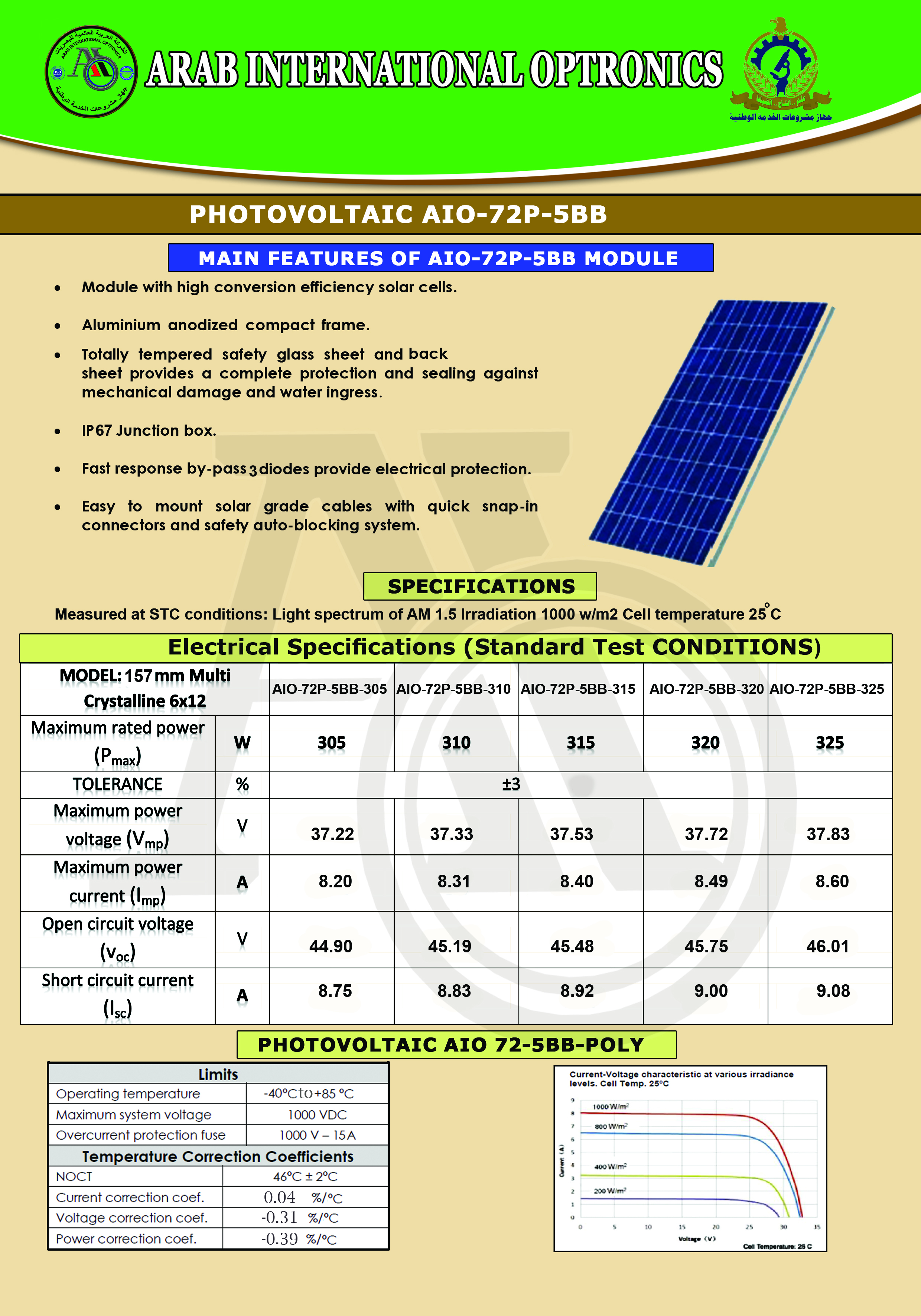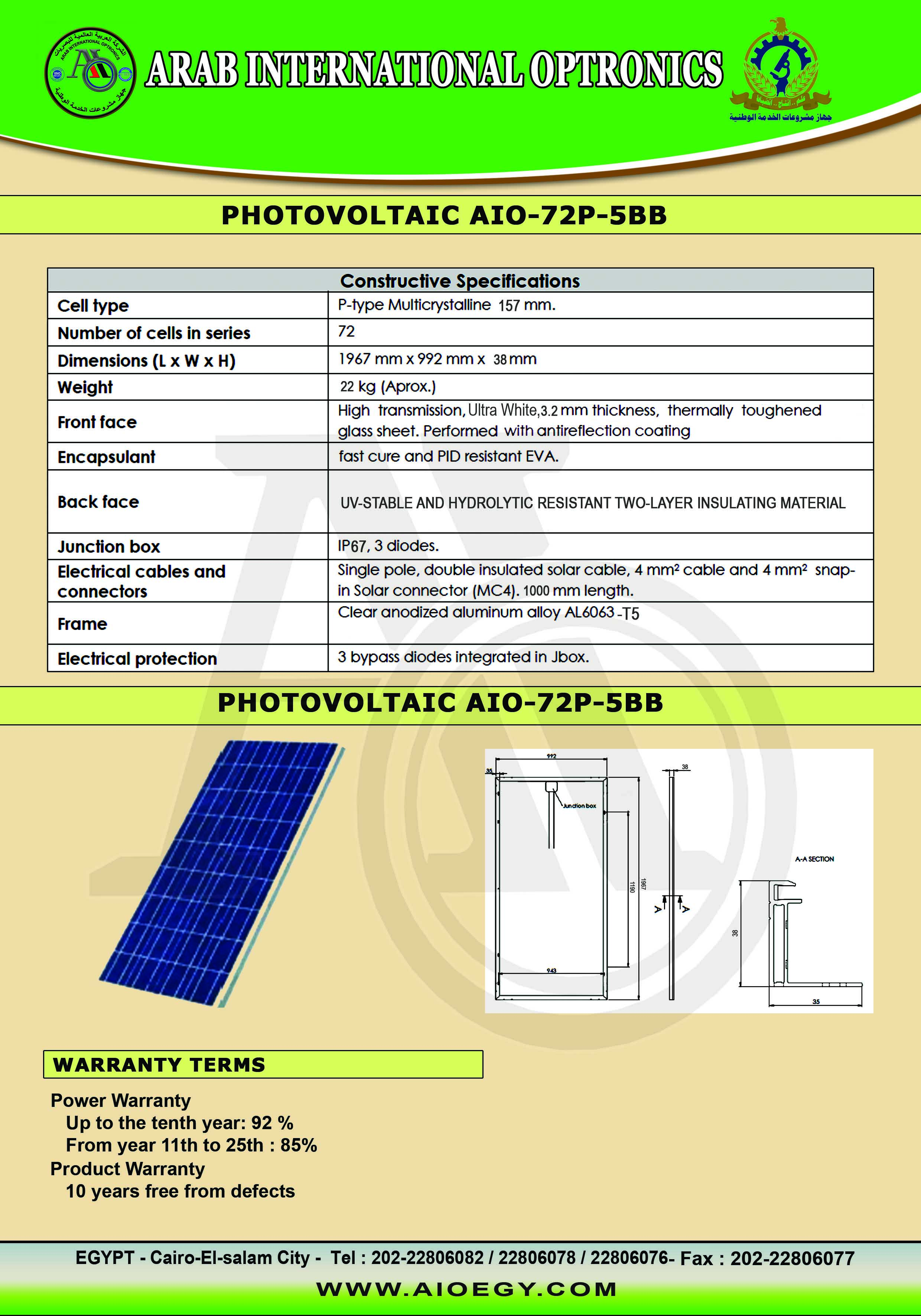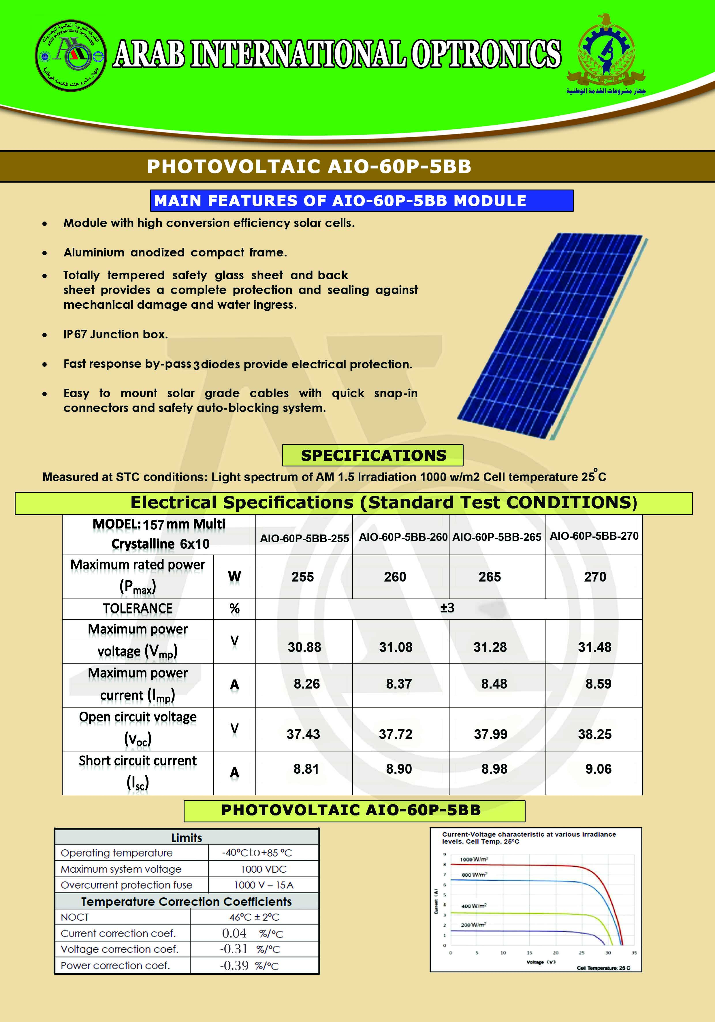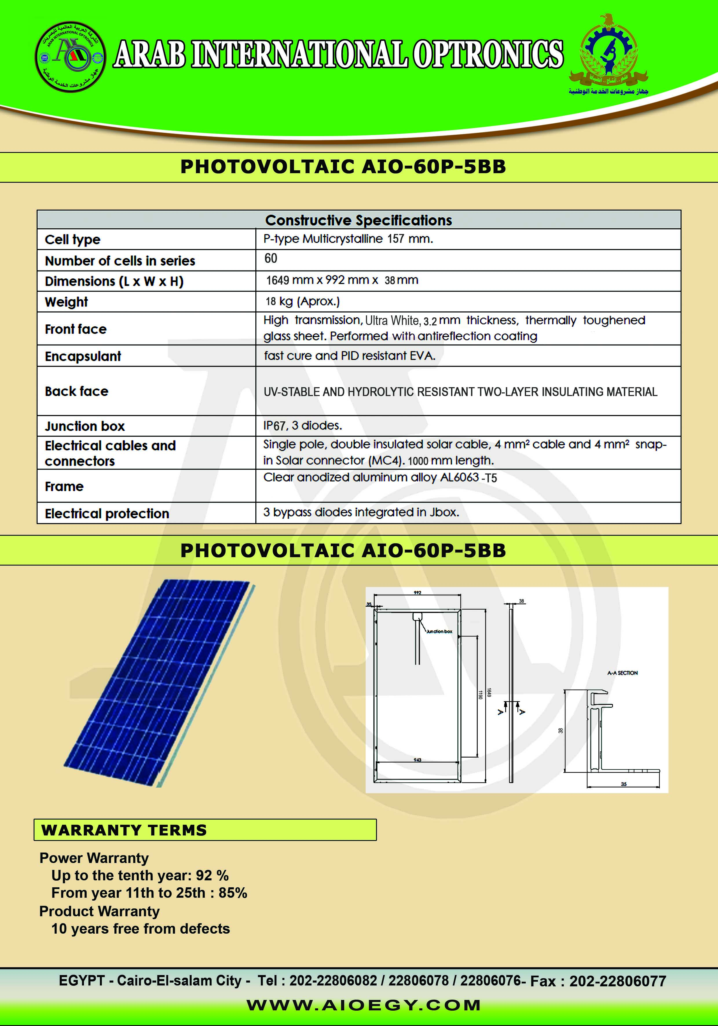
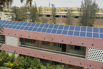
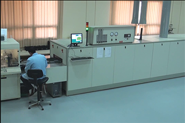


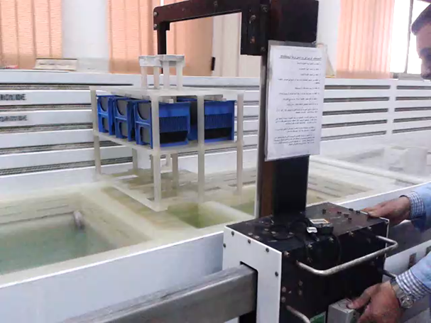
Chemical Lab - Wet Chemistry
Raw silicon wafers are etched in acid baths to surface saw damage from the wafer - cutting processes done at other plants. The etching leaves a series of pyramid structures on the mono-crystalline surface and this assists light absorption.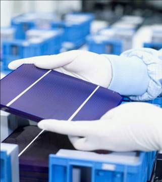
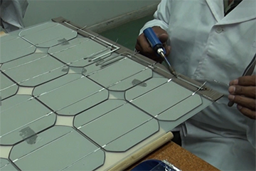
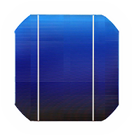
Front Print and Dry
A conductive pattern is screen printed into the front wafer surface with silver-rich paste and then oven belt dried to remove solvents and organic binder residue in the silver paste. The front conductive pattern forms the bus-bar that will conduct the photo-electrons.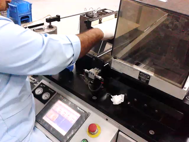
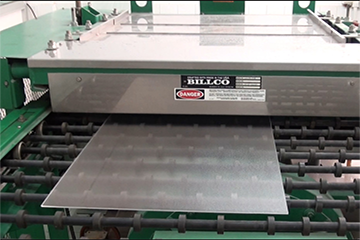
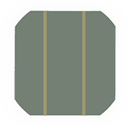
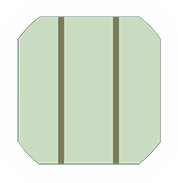
Back Print and Dry
A back print bus-bar is screen printed onto the cell’s rear surface using silver rich paste. The rear busbar provides the means of soldering and interconnecting adjacent cells to make a solar panel.The entire rear surface is screen printed with aluminum, a process called Back Surface Field (BSF).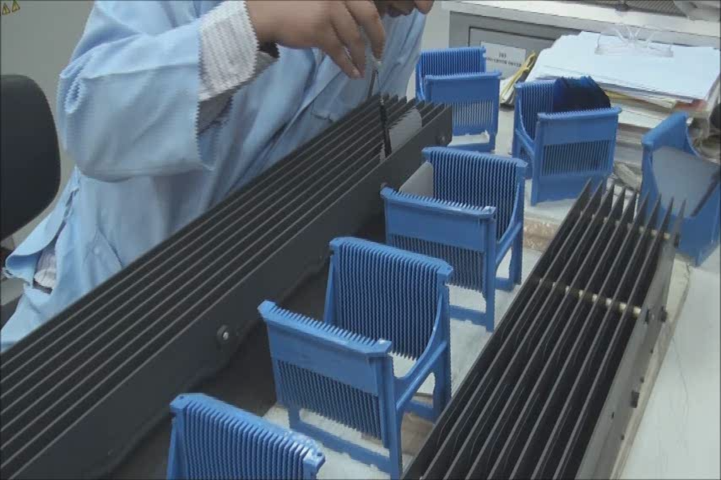
Anti Reflection Coating
A thin anti-reflection (AR) coating of silicon nitride is deposited on the front surface of the wafer using a plasma enhanced vapour deposition process. This AR coating reduces light reflection, increases light absorption, a necessary step to ultimately improve the overall light conversion of the future PV cell.